Выберете то, что вам нужно
-
Этот шаг не переведен. Помогите перевести
-
The iPad camera connection kit. A accessory that many feel does something the iPad should already do.
-
Anyways, here is it torn to pieces (literally), in the interest of seeing what is involved in letting the iPad, which only has a serial and USB interface, talk to a SD Card.
-
-
Этот шаг не переведен. Помогите перевести
-
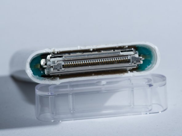
The first step is to even determine how the adapter was assembled, since it has no visible screws.
-
The grey plastic surrounding the dock connector seems to be an insert. Some aggressive prying with a metal spudger caused it to come loose, but not without significantly damaging the plastic housing itself.
-
-
Этот шаг не переведен. Помогите перевести
-
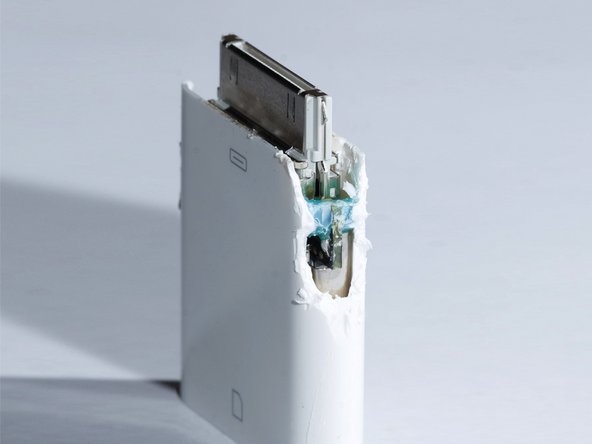
And here we see the reason for the plastic cover's reticence.
-
Apple has chosen to assemble the adapter with epoxy.
-
Effectively, there is no way to non-destructively disassemble the adapter.
-
-
Этот шаг не переведен. Помогите перевести
-
Given that we have already irreparably damaged the plastic casing, the only way forward is through!
-
To gain access to the epoxy bond, we began to shave the sides of the adapter off using an exacto knife or other similar tool.
-
-
-
Этот шаг не переведен. Помогите перевести
-
Other considerations aside, the epoxy is quite brittle. Once the plastic casing was cut back far enough that it could be flexed away from the epoxy blobs, the epoxy bond readily cracked and fragmented.
-
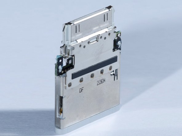
The inner board and SD slot are now free.
-
-
Этот шаг не переведен. Помогите перевести
-
With the casing removed, we see... More barriers!
-
The Circuit board is protected by a metal EMI shield, which is liberally spot-welded in place.
-
This thing is utterly un-repairable. It seems it is designed in the same manner as the magic trackpad, and many of Apple's other recent pieces of small hardware.
-
-
Этот шаг не переведен. Помогите перевести
-
Onward! Spot-welds are generally fairly brittle, and these welds are not very strong, since a truly penetrating weld would likely heat the metal to the point where the plastic parts would melt.
-
Therefore, by forcefully prying, the spot-welded metal components apart, it is possible to break the welds.
-
-
Этот шаг не переведен. Помогите перевести
-
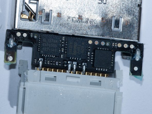
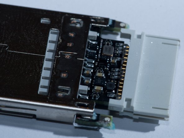
Finally, the circuit board revealed!
-
considering the size of the board, there is a lot of hardware packed on to it.
-
GL137AN GAF0505 022H149 - In a 28 pin QFN package
-
A011 T84V 10MUBB 9J2310 - In a 20 pin QFN package
-
2257 AE072 90K - In a 20 pin QFN package of different origin.
-
Assorted 0402 and 0201 passive components.
-
Testpoints, complete with visible divots from probing during manufacture.
-
-
Этот шаг не переведен. Помогите перевести
-
Finally, the bottom of the interface board. Of interest, what appears to be a small DC-DC converter of unknown purpose. The iPad only supplies 3.3v. For the USB camera connection adapter, a DC-DC converter is required to provide the 5V to run USB devices. However, SD cards run natively on 3.3v, leaving the purpose of the DC-DC a mystery.
-
Tiny package marked only with patterned dots, likely for computer recognition.
-
Little tiny SMT inductor. Unmarked.
-
CEY and some dots. Location near inductor leads to it being likely it is the DC-DC converter IC. 6 Pin package.
-
94F5LF - Very small package, Likely BGA.
-
ET ZD - 4 Pin Package.
-
1200P E06AA - Almost certainly a canned clock oscillator. Probably some permutation of 12 MHz.
-
3 Small 6 pin packages. Pin arrangement leads me to believe they are ferrites or some sort of filter. Probably part of power supply
-
-
Этот шаг не переведен. Помогите перевести
-
After all that, it still works!
-
I wouldn't want to carry it about though, it's too fragile.
-
In the Future: interface protocol. I just need to spend some time with my logic analyzer
-